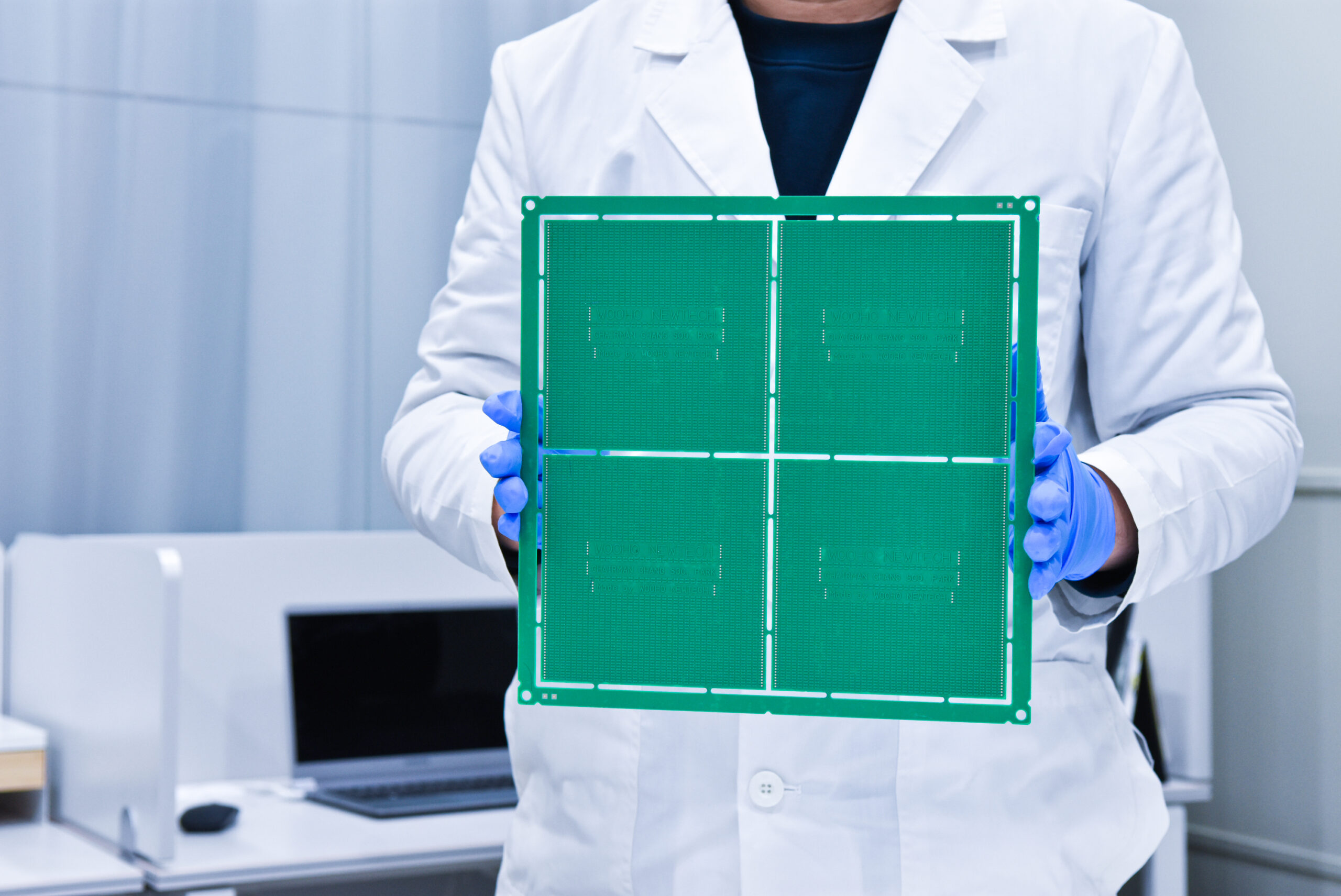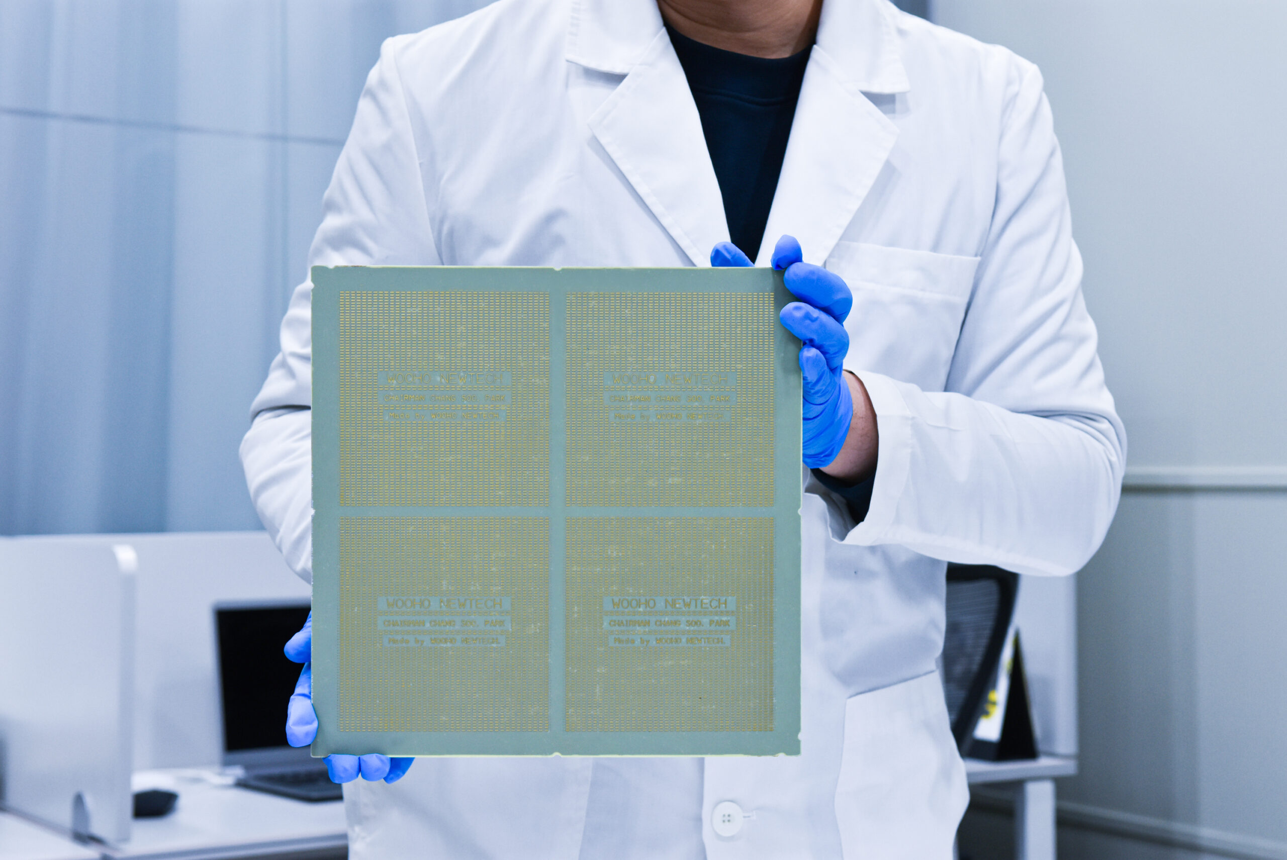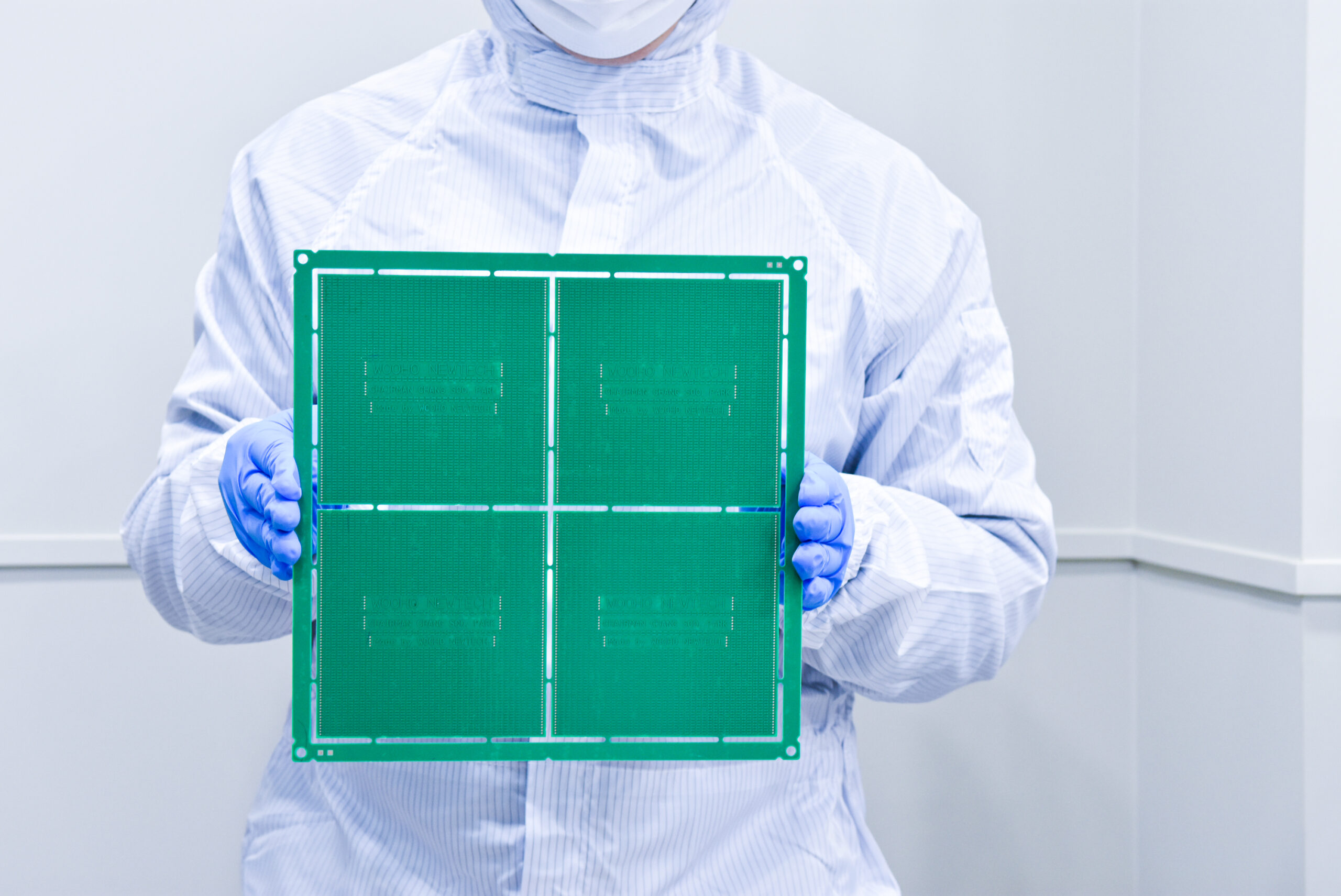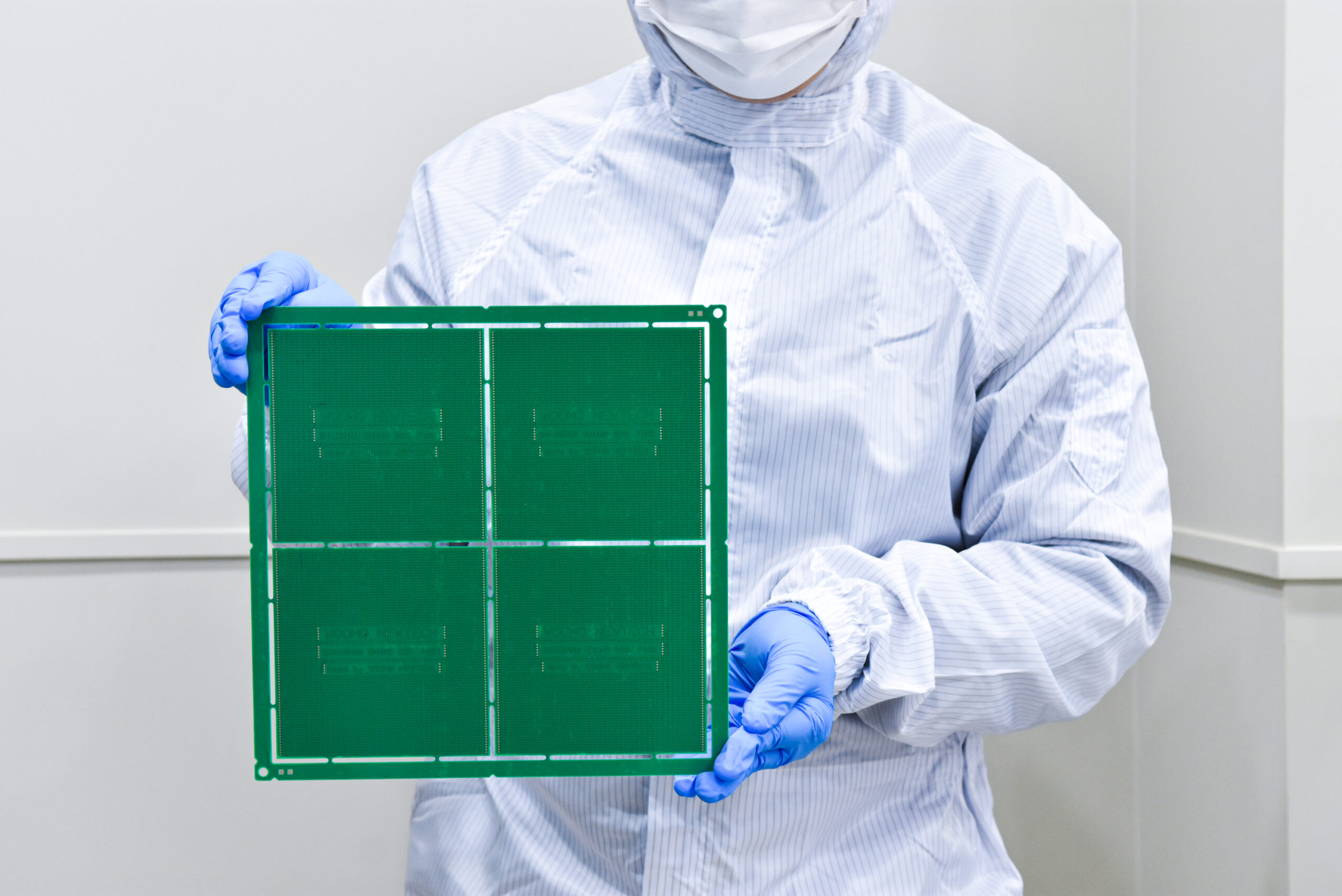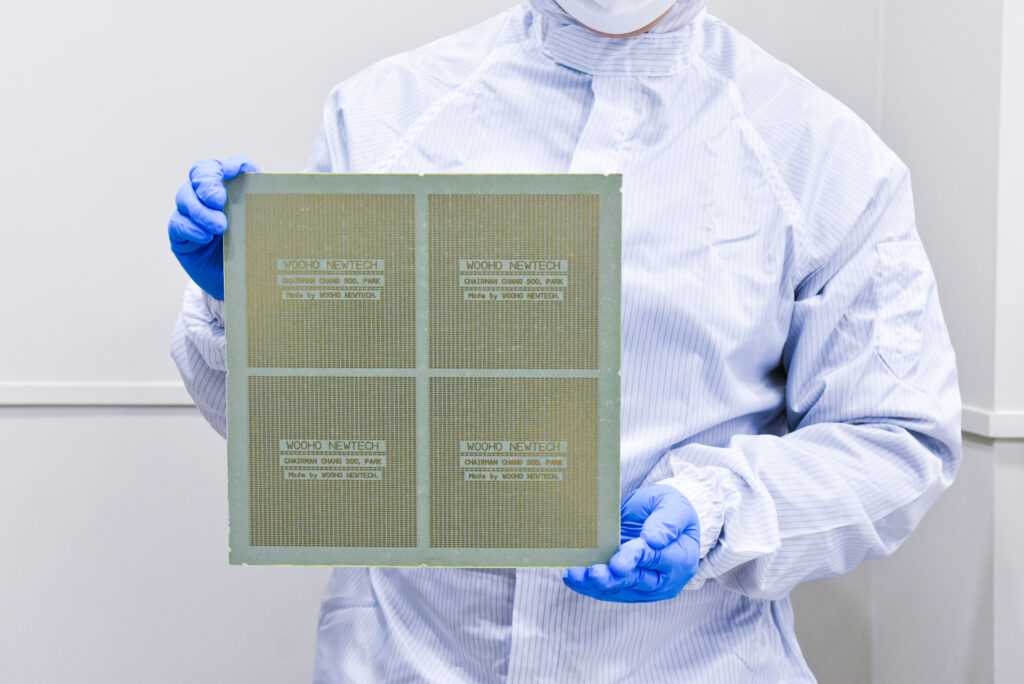
The image shows the newly developed molybdenum-based metal core TMV substrate.
Wooho Newtech Group Develops World’s First
Molybdenum-Based Next-Generation Metal Core Substrate (TMV)
- TMV emerges as a critical enabling technology for AI and HPC semiconductor markets
- Proprietary R&D resolves long-standing challenges in heat dissipation, EMI, large-area panels, and warpage
- Overcomes the fragility and process complexity of glass substrates (TGV), delivering superior mechanical strength and thermal stability
- Expected to drive a paradigm shift in semiconductor packaging
Wooho Newtech Group Co., Ltd., a specialized company in advanced manufacturing design and engineering, announced that it has successfully developed the world’s first molybdenum-based metal core substrate for semiconductors, TMV (Through Metal Via).
Developed entirely through in-house R&D, Wooho Newtech’s molybdenum-based TMV is being recognized as a next-generation substrate technology that fundamentally resolves structural limitations of conventional semiconductor packaging substrates. These include heat dissipation, electromagnetic interference (EMI), large-area panel implementation, substrate warpage, mechanical strength, and high-temperature durability—addressed comprehensively at the material, structural, and process levels.
Limitations of Conventional Substrates in the AI and HPC Era
With the rapid expansion of artificial intelligence (AI), 5G communications, hyperscale data centers, and autonomous driving, the high-performance computing (HPC) semiconductor market is accelerating toward increasingly miniaturized and highly integrated chips.
To keep pace with this trend, the semiconductor industry requires new substrate technologies capable of overcoming the inherent limitations of existing packaging substrates while enabling higher-density interconnections.
In particular, excessive heat generation during high-speed, high-density computation and substrate warpage caused by mismatched coefficients of thermal expansion (CTE) in large-area, multilayer panel structures have emerged as critical industry challenges.
Conventional through-silicon via (TSV) and organic (plastic-based) substrates suffer from poor thermal resistance and severe warpage when scaled to large panel sizes, making them increasingly inadequate for next-generation semiconductor performance requirements.
As a result, the industry has turned its attention to through-glass via (TGV) substrates as a potential alternative to overcome the physical limitations of TSV-based solutions. TGV technology enables vertical electrical interconnections by forming vias through glass substrates, offering high planarity, dimensional stability, and precision circuit implementation. These advantages have positioned TGV as a promising candidate for high-bandwidth memory (HBM), AI semiconductors, and HPC packaging.
However, glass substrates inherently remain highly susceptible to mechanical damage, suffer from significant yield loss at larger panel sizes, and face ongoing challenges in thermal management and EMI shielding.
“Beyond Glass Substrates (TGV)” — The Distinct Advantages of TMV
The molybdenum-based TMV developed by Wooho Newtech Group decisively overcomes the limitations of TGV by employing molybdenum metal as the core substrate material, establishing clear and measurable technical superiority.
Leveraging the exceptional mechanical strength of metal, TMV virtually eliminates breakage risks during manufacturing and enables stable large-area panel processing, delivering significantly higher yields and economic efficiency. In addition, molybdenum exhibits superior thermal conductivity and high-temperature stability compared to glass, enabling highly efficient heat dissipation.
Moreover, the intrinsic properties of metal provide inherent EMI shielding, ensuring robust signal integrity. Molybdenum also possesses a coefficient of thermal expansion closely matched to that of silicon, minimizing warpage and deformation even under high-temperature processing and operating conditions.
Through its molybdenum-based TMV, Wooho Newtech Group has effectively resolved five core challenges:
- Breakthrough heat dissipation performance
- Electromagnetic interference (EMI) shielding
- Large-area substrate scalability
- Suppression of warpage and deformation
- Exceptional mechanical strength and thermal durability
These advantages play a decisive role in maximizing performance stability and extending the operational lifetime of high-performance computing chips.
Future Roadmap
Wooho Newtech Group expects TMV to serve as a foundational technology across next-generation semiconductor applications, including AI accelerators, server-class CPUs and GPUs, autonomous vehicle semiconductors, and 5G/6G communication modules, where extreme reliability and performance are required.
According to leading global market research firms, the advanced semiconductor packaging market is projected to grow at a compound annual growth rate (CAGR) exceeding 10%, reaching approximately USD 100 billion (KRW 130 trillion) by 2030.
A Wooho Newtech Group spokesperson stated,
“Our molybdenum-based TMV solution is a transformative technology capable of redefining the materials and process paradigm of semiconductor packaging. By surpassing the inherent limitations of glass substrates, we aim to secure a uniquely differentiated position in the global semiconductor materials and components market.”
To accelerate commercialization, Wooho Newtech Group plans to establish a complete TMV value chain by collaborating with global semiconductor companies and AI/HPC ecosystem partners. The company will actively pursue joint reliability testing, pilot line development, and mass-production partnerships, while continuing to expand R&D into next-generation TMV processes.